/// Research
Projects
/Topics ///
GRANTS RECEIVED
-
Principal
Investigator, CDS&E: Coupled Thermal, Piezoelectric, and
Hot Carrier Effects in AlGaN/GaN HEMTs: Multiscale Modeling
of Time Evolution of Device Degradation, National Science
Foundation (NSF), award no. 1610474, funds received
$282,815, 9/1/2016–8/31/2019.
-
Co-Principal
Investigator, Design of Gallium Oxide Based Wireless
Smart Sensor Platform for In-situ Oxygen Monitoring in
Coal-Fired Power Plants, SIU Energy Boost Seed Grant,
(PI: Chao Lu) funds received: $50,000, 2018-19.
-
Co-Principal
Investigator, Novel Chalcogenide Derivatives for
Thermoelectric Energy Conversion (PI: Thushari Jayasekera),
funds received: $20,000, SIU MTC Seed Grant
(1/1/2015-5/15/2016).
-
Senior Personnel,
NSF DMR: REU Site in Interdisciplinary Materials Research,
National Science Foundation (NSF), (PI: Boyd
Goodson), award no. 1461255, funds received: $330,000,
Period: 4/1/2015 – 09/1/2017.
-
Principal Investigator,
NSF Research Experience for Undergraduates (REU) Supplement
(NSF SHF: Embedded cooling of high-performance ICs using
Novel nanostructured thermoelectrics: Multiscale Software
development and device optimization), National Science
Foundation (NSF), award no. 1442021, funds received
$16,000, 7/1/2014–6/30/2016.
-
Principal Investigator,
SHF: Embedded cooling of high-performance ICs using Novel
nanostructured thermoelectrics: Multiscale Software
development and device optimization, National Science
Foundation (NSF), award no. 1218839, funds received
$149,921, 7/1/2012–6/30/2016.
-
Principal Investigator,
Multiscale computational studies on the degradation
mechanisms in nanoscale nitride-based HEMT devices, User
Nanoscience Research Program Award, DOE Oak Ridge
National Laboratory, award no. CNMS2011-228,
collaboration time with a research scientist (valued $20,720
by ORNL) and access to HPC platforms, 8/1/2011–7/31/2012.
-
Principal Investigator,
Role of coupled structural-thermal-material processes in the
failure mechanism of a high-speed bearing assembly,
United Technologies and Center for Embedded Systems (CES),
funds received: $25,000, 8/16/2011–8/15/2012, co-PI: Jun
Qin, Philip Chu.
-
Principal Investigator,
ECCS: Fundamental studies of efficiency droop in III-nitride
solid-state lighting devices, National Science Foundation
(NSF), award no. 1102192, funds received: $252,329,
8/1/2011–7/31/2016.
-
Co-Principal
Investigator, Partnership for improved achievement in
science through computational science, PI: Frackson Mumba,
co-PIs: Mesfin Tsige, Michelle Zhu, Kevin Wise, Illinois
State Board of Education (ISBE), funds received:
~$530,000, 7/2010 -9/2012.
-
Principal Investigator,
Modeling bandstructure effects in nanoscale solid-state
lighting devices, SIU Faculty Research Grant,
funds: $19,176 (7/1/2010–6/30/2011)
-
Principal Investigator,
Southern Illinois HPC Infrastructure (SIHPCI), National
Science Foundation (NSF), award no. 0855221, funds
received: $360,779.00, 9/1/2009–8/31/2012 [co-PIs: Mark
Byrd, Tony Oyana, Qiang Cheng, Mesfin Tsige].
-
Principal Investigator,
Multimillion-Atom Modeling of Nanoelectronic Materials and
Devices for Harsh Environments, DOE Oak Ridge National
Laboratory and ORAU, funds received: $75,000 and access
to ORNL supercomputing platforms, 5/15/2009–5/14/2012.
Theory/Models/Algorithms
|
Novel NEGF algorithms
:
The Non-Equilibrium
Green’s Function (NEGF) approach is considered as the
state-of-the-art modeling tool for predicting performance and
designing emerging nanoscale devices. However, accurate and reliable
modeling of the future nanoscale devices requires huge computational
efforts, yet the current NEGF algorithms are prohibitively
expensive. Collaborated with Stanford University, NASA Ames,
University of Alabama, and Purdue University for the development and
implementation of novel algorithms and methodologies for the
calculations of non-equilibrium Green’s functions and associated
charge densities from large sparse matrices describing the
underlying nanoscale systems. Different parallel computing
methodologies using MPI and OpenMP were studied and implemented in
these application software for achieving optimum speed/memory
performance.
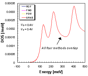
[S. Li, S. Ahmed, E. Darve, and G.
Klimeck, "Compute the Diagonal of Sparse Matrix Inverse using FIND
Algorithm", Journal of Computational Physics, Vol. 227, pp.
9408–9427, 2008]
|
|
|
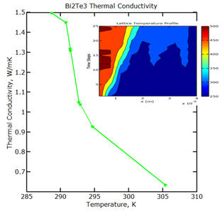
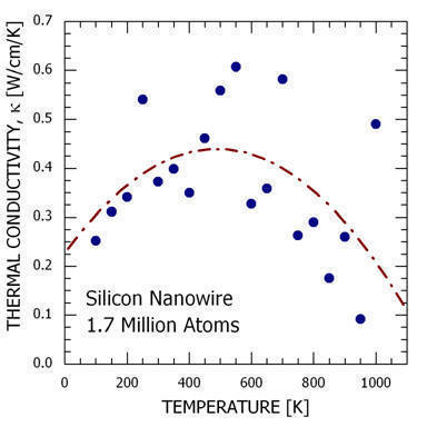
Full-Band
Particle-Based Monte-Carlo Simulation with Anharmonic Corrections
for Phonon Transport: Monte Carlo based statistical
approach to solve Boltzmann Transport Equation (BTE) has become a
norm to investigate heat transport in semiconductors at sub-micron
regime, owing to its ability to characterize realistically sized
device geometries qualitatively. One weakness of this technique is
that the approach predominantly uses empirically fitted phonon
dispersion relation as input to determine the properties of phonons
and predict the thermal conductivity for a specified material
geometry. The empirically fitted dispersion relations assume
harmonic approximation, thereby failing to account for thermal
expansion, effects of strain on spring stiffness, and accurate
phonon-phonon interactions. To account for the anharmonic
contributions in the calculation of thermal conductivity, in this
work, we employ a coupled molecular mechanics-Monte Carlo (MM-MC)
approach. The atomistically-resolved non-deterministic approach
adopted in this work is found to produce satisfactory results on
heat transport and thermal conductivity in both ballistic and
diffusive regimes for III-N nanostructures. Figure on right shows
the lattice thermal conductivity of Bi2Te3 thin film, inset
illustrating how temperature distribution in the device active
region evolves with time. (Supported by the U.S. National Science
Foundation) |
 |
|
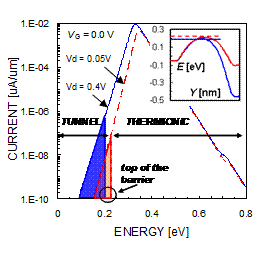
Quantum potential :
Worked in the development of a
parameter-free quantum field approach for use in conjunction with particle-based
simulations. The method is based on a perturbation theory around thermodynamic
equilibrium and leads to a quantum field formalism in which the size of an
electron depends upon its energy. The approach when used in the simulations of a
conventional nanoscale 25 nm n-channel MOSFET device
is found to produce correct experimentally verified threshold voltage shifts of
about 220 mV and drain current degradation of about 30%. To further test the
applicability, the quantum field formalism is used to calculate the threshold
voltage and output characteristics of recently proposed single-gated (SG) and
dual-gated (DG) fully-depleted silicon-on-insulator (FDSOI) devices. It is
observed that the method quite correctly retrieves the trend in the threshold
voltage shift with the variation of silicon film thickness. The simulation
results are verified with the available experimental and/or theoretical data.
[Shaikh Ahmed, Christian Ringhofer, and Dragica
Vasileska, “Parameter-Free Effective Potential Method for Use in Particle-Based
Device Simulations”, IEEE Transactions on Nanotechnology, Vol. 4, 4, pp.
465–471, 2005. ]
|
Quantum
barrier potential in an FET device |
|
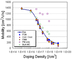
Fast Multipole Method (FMM)
:
In a typical particle-based
device simulation experiment, a drawback is that the
3-D Poisson equation must be solved repeatedly to properly describe the
self-consistent fields, which consumes over 80% of the total simulation time. To
further speed up simulations, we used a 3-D Fast Multi-Pole Method (FMM)
instead. The FMM allows calculation of the field and the potential in a system
of n particles connected by a central force within
operations given certain prescribed accuracy. The FMM is based on the idea of
condensing the information of the potential generated by point sources in
truncated series expansions. After calculating suitable expansions, the long
range part of the potential is obtained by evaluating the truncated series at
the point in question and the short range part is calculated by direct
summation. The field due to the applied boundary biases is obtained at the
beginning of the simulation by solving the Poisson equation. Hence the total
field acting on each electron is the sum of this constant field and the
contribution from the electron-electron and electron-impurity interactions
handled by the FMM calculations. The image charges, which arrive because of the
dielectric discontinuity, are handled by the method of images.
The correctness of the approach is verified via the simulations of the doping
dependence of the low-field electron mobility in a 3-D resistor and its
comparison with available theoretical and experimental data.
[L. Greengard and V. Rokhlin, “A
fast algorithm for particle simulations,” J. Comp. Phys., Vol.
135, no. 2, pp. 280–292, 1997]
[H. Khan, S. Ahmed, and D.
Vasileska, C. Heitzinger, C. Ringhofer, “Modeling of FinFET: 3D
MC Simulation Using FMM and Unintentional Doping Effects on
Device Operation”, Journal of Computational Electronics, Vol. 3,
pp. 337–340, 2004]
[D. Vasileska and S. Ahmed,
“Narrow-Width SOI Devices: The Role of Quantum Mechanical Size
Quantization Effect and the Unintentional Doping on the Device
Operation”, IEEE Transactions on Electron Devices, Vol. 52,
Issue 2, pp. 227–236, 2005]
|
|
|
Event-biasing for statistical enhancement in the Monte-Carlo device simulations : Enhancement
algorithms are especially useful when the device
behavior is governed by rare events in the carrier
transport process. It is shown that the weight of the
particles, as obtained by biasing the Boltzmann
equation, survives between the successive steps of
solving the Poisson equation. Particular biasing
techniques are applied to the simulations of
subthreshold conduction in a 15 nm n-channel MOSFET and
the convergence of both the terminal current and the
channel current is analyzed.
It is found that
event-biasing experiments recover precisely the physical
averages and the self-consistent field and reduces the
time necessary for computation of the desired device
characteristics.
[Shaikh
Ahmed, Mihail Nedjalkov, and Dragica Vasileska, “Comparative
Study of Various Self-Consistent Event Biasing Schemes for Monte
Carlo Simulations of Nanoscale MOSFETs,” In Theory and
Applications of Monte Carlo Simulations, book edited by
Victor (Wai Kin) Chan, ISBN 978-953-51-1012-5, Published: March
6, 2013.]
[M. Nedjalkov, S. Ahmed, and D.
Vasileska, “A self-consistent event biasing scheme for
statistical enhancement”, Journal of Computational Electronics,
Vol. 3, pp. 305–309, 2004]
|
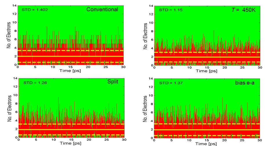
Enhancement of
Statistics: Reducing Standard Deviation |
|
Parallel computation.
Parallel
programming and algorithms are parts and parcels in our group and routinely
used. Parallel applications like LAMPS and NEMO 3-D are the core components in
the software developed by the group. LAMMPS is a classical molecular dynamics
code that models an ensemble of particles in a liquid, solid, or gaseous state.
It can model atomic, polymeric, biological, metallic, granular, and
coarse-grained systems using a variety of force fields and boundary conditions.
LAMMPS is designed to be easy to modify or extend with new capabilities, such as
new force fields, atom types, boundary conditions, or diagnostics. Excellent
parallel scaling exceeding 120,000 cores has recently been performed by our
group on ORNL Jaguar XT5, maximum number of atoms simulated being ~3.84 billion!
Also, In the self consistent quantum simulations, the most computationally
expensive part is the Green’s function calculation at every energy point. For
example, the size of the Hamiltonian can be up to 7000×7000, block-tri-diagonal.
Depending on the required energy resolution, the equations may need to be solved
1000 times for every Poisson iteration. In order to reduce the computational
burden, the MPI (message passing interface) parallelization scheme has been
implemented in most of the quantum transport solvers in the independent
computation of Green’s function at each point along the energy spectrum.
|
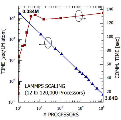
LAMMPS scaling in Cray XT5 machine at ORNL
|
go to top
Devices and Phenomena
|
Electronic structure of realistically-sized quantum dots
: The theoretical knowledge of the electronic structure
of nanoscale semiconductor devices is the first and most essential
step towards the interpretation and the understanding of the
experimental data and reliable device design at the nanometer scale.
Electronic band structure of a solid originates from the wave nature
of particles and depicts the allowed and forbidden energy states of
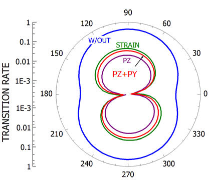
electrons in the material. Recently we have studied symmetry
breaking and energy level splitting in self-assembled Zincblende and
Wurtzite quantum dots through atomistic simulations. The symmetry in
quantum dots realized from III-V materials is lowered due to two fundamental
symmetry breaking mechanisms: (a) the underlying crystal, which
lacks inversion symmetry, (2) the presence of strain, and (3) strain
induced piezoelectric potential. In III-N materials, in addition to
piezoelectric field, there exists a pyroelectric contribution as
well. Results show a significant dependence of the dot states and
optical polarization on the geometry (Box/Dome/Pyramid) and size of
the QDs.
NEMO 3-D, a versatile
and open source electronic structure code that can handle device
domains relevant for realistic large devices, is used in this work.
Realistic devices containing millions of atoms can be computed with
reasonably, easily available cluster computers. NEMO 3-D employs a
VFF Keating model for strain and the 20-band sp3d5s*
empirical tight-binding model for the electronic structure
computation. It is released under an open source license and
maintained by the NCN at Purdue University, West Lafayette under the
supervision of
Professor Gerhard Klimeck.
|
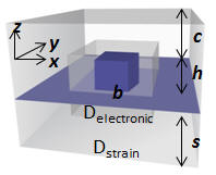
|
Quantum dots on a thin (one
atomic layer) InAs wetting layer. Two major
computational domains are also shown. Delec: central
smaller domain for electronic structure (quantum)
calculation, and Dstrain: outer domain for strain
calculation. In the figure: s is the substrate height, c
is the cap layer thickness, h is the dot height, and d
is the dot diameter/base length as appropriate. |
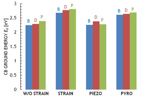
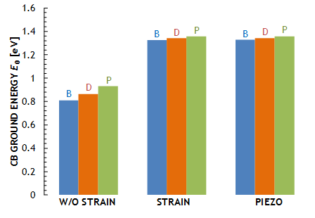
Conduction band ground states in box (B), dome (D), and
pyramid (P) shaped InN/GaN quantum dots including
interface effects (w/out strain), strain,
piezoelectricity, and pyroelectricity. |
|
Conduction band ground states in box (B), dome (D), and
pyramid (P) shaped InAs/GaAs quantum dots including
interface effects (w/out strain), strain, and
piezoelectricity.
|
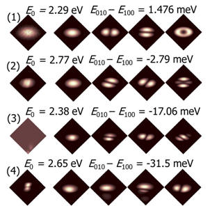
Topmost
valence band
and
first 4 Conduction band wavefunctions in dome shaped InN/GaN quantum dots
including (1) interface effects, (2) strain, (3)
piezoelectricity, and (4) pyroelectricity.
|
|
[Shaikh Ahmed, Sharnali Islam, and
Shareef Mohammed, “Electronic Structure of InN/GaN Quantum Dots:
Multimillion Atom Tight-Binding Simulations”,
special issue of IEEE Transactions on Electron
Devices on LEDs, vol. 57, 1, pp. 164–173, January 2010]
[Shaikh Ahmed, Neerav Kharche, Rajib Rahman, Muhammad Usman,
Sunhee Lee, Hoon Ryu, Hansang Bae, Steve Clark, Benjamin Haley,
Maxim Naumov, Faisal Saied, Marek Korkusinski, Rick Kennel,
Michael Mclennan, Timothy B. Boykin, and Gerhard Klimeck,
“Multimillion Atom Simulations with NEMO 3-D”, In Meyers, Robert
(Ed.) Encyclopedia of Complexity and Systems Science, Vol. 6, pp
5745–5783. Springer New York 2009]
[Gerhard Klimeck, Shaikh Ahmed, Neerav
Kharche, Hansang Bae, Steve Clark, Benjamin Haley, Sunhee Lee, Maxim
Naumov, Hoon Ryu, Faisal Saied, Marta Prada, Marek Korkusinski, and
Timothy B. Boykin, “Atomistic Simulation of Realistically Sized
Nanodevices Using NEMO 3-D: Part I–Models and Benchmarks”, IEEE
Transactions on Electron Devices, Vol. 54, 9, pp. 2079–89, 2007]
[Gerhard Klimeck, Shaikh Ahmed, Neerav
Kharche, Marek Korkusinski, Muhammad Usman, Marta Prada, and Timothy
Boykin, “Atomistic Simulation of Realistically Sized Nanodevices
Using NEMO 3-D: Part II–Applications”, IEEE Transactions on
Electron Devices, Vol. 54, 9, pp. 2090–99, 2007] |
|
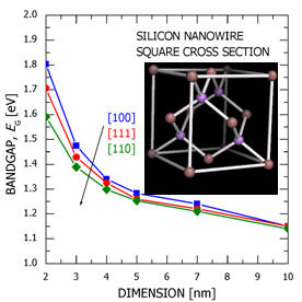
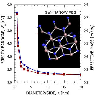
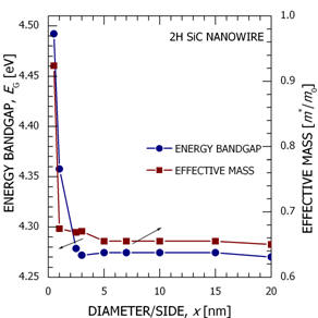
Atomistic electronic structure of ZB and WZ nanowires :
In the last decade,
nanowires (NWs) made from a wide variety of materials have drawn
considerable interest because of their potential applications in
various optoelectronic and high-mobility electronic devices. Using
NWs in these devices, the performance is enhanced due to increased
charge localization and reduction in the defect density. In this
work, electronic bandstructure of [0001]-oriented Wurtzite nanowires
with square cross sections is calculated using sp3s*d5 and sp3s*
tight-binding models and then used to parameterize the bandgap and
Gamma-valley effective masses. The materials used include: group
III-V, group III-nitrides, group II-VI (CdSe, ZnSe, CdS and ZnS) and
2H-SiC. |
|
 |
 |
 |
 |
|
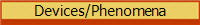
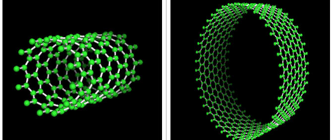
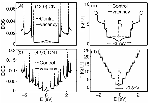
Carbon nanotubes. The electronic behavior of metallic carbon nanotubes
under the influence of atomistic vacancy defects present in the
channel is theoretically investigated using the Non-Equilibrium
Green’s function (NEGF) method self-consistently coupled with
three-dimensional (3D) electrostatics. A nearest neighbor tight
binding model based on a single pz orbital is used for the device
Hamiltonian. A single vacancy defect in the channel of a small
diameter metallic carbon nanotube can decrease its conductance by a
factor of two. More than one vacancy in the channel can further
drastically decrease the conductance. Larger diameter nanotubes
suffer less from the presence of vacancy defects. The presence of a
single vacancy locally modulates the LDOS significantly in the
device. More importantly, regardless of the chirality of the
nanotube, the transmission is reduced throughout the entire energy
spectrum (by one quantum unit in some regions). The work is done in
collaboration with Neophytos Neophytou and Gerhard Klimeck at Purdue
University.
[N. Neophytou, S. Ahmed, G.
Klimeck, “Influence of vacancies on metallic nanotube transport
performance”,
Applied Physics Letter, 90, 182119, 2007]
|
|
 |
 |
|
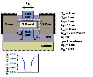
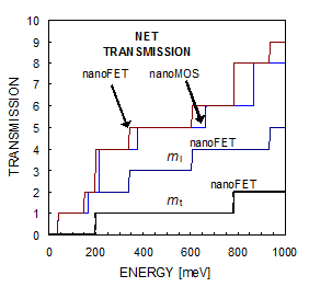
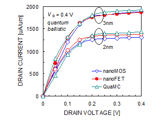
Quantum simulations of
nanoscale dual-gate
MOSFETs.
There is a virtual consensus that the most practically scalable
variety of all novel MOSFETs, that are in the focus of many
researchers’ study today, are the double-gate SOI MOSFETs with a
sub-10 nm gate length, ultra-thin, intrinsic channels and highly
doped (degenerate) bulk electrodes. In such transistors, short
channel effects typical for their bulk counterparts are minimized,
while the absence of dopants in the channel maximizes the mobility
and hence drive current density. Such advanced MOSFETs may be
practically implemented in several ways including planar, vertical,
and FinFET geometries. However, several design challenges have been
identified such as a process tolerance requirement of within 10% of
the body thickness and an extremely sharp doping profile with a
doping gradient of 1 nm/decade. The SIA forecasts that this new
device architecture may extend MOSFETs to the 22 nm node (9-nm
physical gate length) by 2016. Intrinsic device speed may exceed 1
THz and integration densities will be more than 1 billion
transistors/cm2.This work focused mainly on the modeling
and simulations of the size-quantization effect within a fully
quantum mechanical Non-equilibrium Green’s Function (NEGF)
approach and a quantum-corrected Monte Carlo transport framework
for 2-D MOSFET structures and presents benchmark results of three
software packages namely nanoFET, nanoMOS and QuaMC 2-D.
[Shaikh Ahmed, Gerhard Klimeck,
Derrick Kearney, Michael McLennan, MP Anantram, “Quantum
Simulations of Dual Gate MOSFET Devices: Building and Deploying
Community Nanotechnology Software Tools on NanoHUB.org”, Journal
of High Speed Electronics, Vol. 17, 3, pp 485–494, 2007]
|
 |
|
|
 |
|
Unintentional /discrete dopant effects in Si nanowires
:
Numerical simulations
are performed to study the single-charge-induced ON-current
fluctuations (random telegraphic noise) in silicon nanowire
field-effect transistors. A 3-D fully atomistic quantum-corrected
particle-based Monte Carlo device simulator (MCDS 3-D) has been used
in this work. Our study confirms that the presence of single channel
charges modifies the electrostatics (carrier density) and dynamics
(mobility) of the device, both of which play important roles in
determining the magnitude of the current fluctuations. The relative
impact (percentage change in the ON-current) depends on an intricate
interplay of device size, geometry, channel (crystal) orientation,
gate bias, and energetics and spatial location of the charge.
[Ramya Hindupur, Sharnali Islam,
and Shaikh Ahmed, "Atomistic Modeling of Unintentional Single
Charge Effects in Silicon Nanowire FETs," Technical Proceedings
of IEEE Nanotechnology Materials and Devices Conferences (NMDC)
2010, October 12-15, pp. 282-285, California, USA]
|
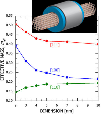
Gamma-valley effective mass as a function
of the cross-sectional dimension of silicon nanowire. |
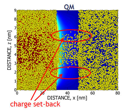
Electron
distribution in the active region.
|

Energy
plot for VG
= VD = 0.8 V when a single impurity is
present at the source-end of the channel. |
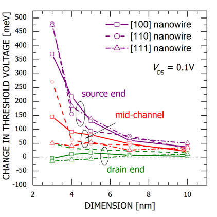
Comparison of percentage change in the
threshold volatge due to the presence of a single
negative charge in [100], [110], and [111] silicon
nanowires. |
|
Modeling Random Dopant Fluctuation Effects in Nanoscale Tri-Gate
MOSFETs.
The tri-gate FET has been hailed as the biggest
breakthrough in transistor technology in the last 20 years. The
increase in device performance (faster switching, low power,
improved short channel effects, etc.), coupled with the reduction in
device size, would allow for huge gains in the electronics industry.
In this work, an atomistic quantum-corrected Monte Carlo 3-D device
simulator was used to not only investigate the validity of these
claims, but also how quantum size quantization and random dopant
fluctuation (RDF) affect the tri-gate FET performance and how to
curb these issues. The main findings are as follow: 1) carrier
scattering leads to ON current degradation of ~30% and hence cannot
be ignored; 2) deviations in threshold voltage due to random channel
doping are smaller in the tri-gate FET; 3) RDF due to the
source/drain discreteness can be engineered by adjusting the
source/drain junction depth. With randomness reduced, the overall
performance should increase when used in ICs, where consistency in
device characteristics is essential. |
|
Self-heating in silicon-on-insulator FETs :
|
|
 |
 |
 |
|
Bandstructure
and crystal orientation effects in III-V MOS devices.
Nanoscale double-gate n-MOSFETs with silicon and III-V (GaAs and
InAs) channels are studied using numerical simulation. The device
structures are based on the ITRS 14nm node (year 2020), and are
simulated using the program nanoMOS, which utilizes the NEGF
technique for treating ballistic electron transport in the
channel. The effective masses used are obtained by extraction from
the full band structure using the sp3d5s*
empirical tight-binding method. This process returns effective mass
values for all valleys which are far more accurate than bulk values
for the ultra-thin-body MOSFET. The results indicate that for
digital logic applications, III-V materials offer little or no
performance advantage over silicon for ballistic devices near the
channel length scaling limit.
[Himadri S. Pal, Kurtis D. Cantley,
Shaikh S. Ahmed, and Mark S. Lundstrom, "Influence of Bandstructure
and Channel Structure on the Inversion Layer Capacitance of Silicon
and GaAs MOSFETs", IEEE Transactions on Electron Devices,
vol. 55,
issue 3, pp 904–908, 2008] |
|
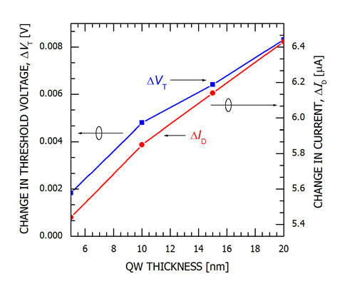
Modeling Floating Body Memory
Devices.
Numerical simulations using
the Silvaco TCAD tool have been performed to model
dual-gate floating body ZRAM devices. Floating body
memories are a new generation memory cells which are
being researched as an alternative for DRAM memory in
order to get rid of the bulky storage capacitor. The
states are written into the device using impact
ionization to generate a large number of holes in the
substrate, which alter the threshold voltage of the
device. Amongst a group of variants, dual gate
structures help reduce drain-induced barrier lowering
and hence leakage, while having better control of the
charge in the substrate. In addition to the bulk
DG-ZRAM cell, a recently proposed DG-ZRAM structure with
a SiGe quantum well (QW) introduced into the substrate
(which acts as a hole storage pocket) was also
simulated. Comparisons in terms of noise margin
(∆ID) have been made for both the
devices, which show that the structure with the QW in
the substrate performs better than the bulk structure.
For the QW cell, simulations have been performed taking
into consideration gate electrodes with different work
functions and it has been observed that while aluminum
has a detrimental impact in conventional MOSFETs due to
high off-state leakage current, it can be used to obtain
low power ZRAM memory cells. Parameters such as QW
doping density, composition, channel length, QW
thickness and its position from the top gate have been
varied to obtain the optimum noise margin for the
device.
[Ramya Hindupur and Shaikh
Ahmed] |
 |
 |
|
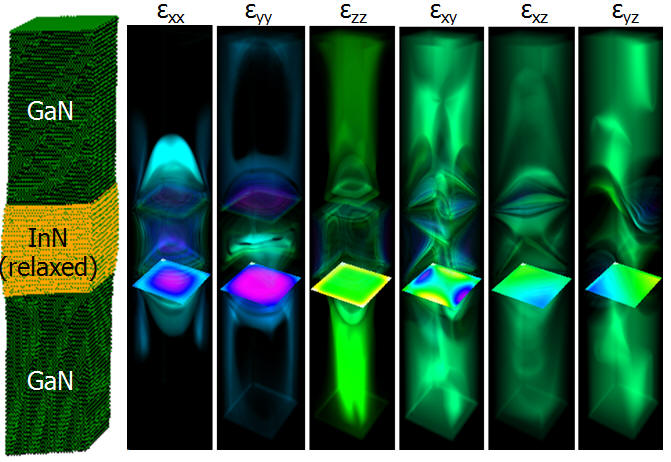
Atomistic Modeling of Degradation Mechanisms in Nanoscale HEMT
Devices.
Through atomistic numerical simulations, we
investigate how performance degradation of state-of-the-art AlGaN
HEMTs is governed by an intricate coupling of the underlying
thermo-electro-mechanical processes while operating at high power
and/or high-temperature. The polarization induced charge density is
shown to be strongly dependent on the thickness of the AlN barrier
layer. This further demonstrates that the degradation in these HEMT
devices is related to the reduction of the effective thickness of
the AlN barrier layer, which, during operation at high device
temperature, could arise from the diffusion of gate metal into the
barrier material matrix. This finding has been validated using the
massively parallel LAMMPS molecular dynamics tool and available
experimental data. We have also demonstrated that the polarization
fields alone can induce channel carriers at zero external bias and
lead to a significant increase in the ON current. |
Nanoscale devices
for energy-related applications:
|
Modeling
droop in solid-state lighting devices
: III-nitride
solid-state lighting (SSL) has the potential, by 2025, to decrease
electricity consumed by lighting by >50%, cut ~28 million metric
tons of carbon emission annually, and benefit general illumination,
transportation, communication, automobiles, imaging, agriculture,
and medicine. SSL will revolutionize semiconductor market and can
reestablish U.S. manufacturing leadership. The objective of this
research is to computationally investigate: i) how efficiency droop
and color degradation in III-nitride SSL devices are governed by an
intricate interplay of crystal atomicity, built-in structural
fields, and charge and phonon transport processes, and ii) how
tuning the basic physical properties at nanoscale can create
transformative solution paths. [Supported by NSF]
[Md.
Rezaul Karim Nishat, Mayada M. Taher, and Shaikh S. Ahmed,
“Million-Atom Tight-Binding Modeling of Nonpolar
a-Plane InGaN Light
Emitters," Journal of
Computational Electronics, vol. 17, no. 4, pp. 1630–1639,
2018.
Mayada Taher and Shaikh Ahmed, “III-Nitride Multiple Disk-in-Wire
Laser Structures: Effects of Crystal Orientation and Spacer Size,”
Optical Materials, vol. 83,
pp. 104–110, 2018.
Md Rezaul Karim Nishat, Saad M. Alqahtani, Vinay U. Chimalgi, Neerav
Kharche, and Shaikh S. Ahmed, “Atomistic Modeling of Nonpolar
m-Plane InGaN Disk-in-Wire
Light Emitters,” Journal of
Computational Electronics, vol. 16, no. 3, pp. 814–824, 2017.
Saad Mubarak Al-Qahtani, Abdulmuin Abdullah, Md. Rezaul Karim Nishat
and Shaikh Ahmed, “Diameter
Dependent Polarization in ZnO/MgO Disk-in-Wire Emitters:
Multiscale Modeling of Optical Quantum Efficiency,”
Superlattices and Microstructures,
vol. 103, pp. 48–55, 2017.
Vinay Chimalgi, Md. R. K. Nishat, and Shaikh Ahmed, “Nonlinear
Piezoelectricity and Efficiency
Droop in Hexagonal In(Ga)N/GaN Disk-in-Wire LEDs,”
Superlattices and Microstructures,
vol. 84, pp. 91–98, 2015.
Shaikh Ahmed, Sasi Sundaresan, Hoon Ryu, and Muhammad Usman,
“Multimillion-Atom Modeling of InAs/GaAs Quantum Dots: Interplay of
Geometry, Quantization, Atomicity, Strain, and Linear and Quadratic
Polarization Fields,” Journal of
Computational Electronics, vol. 14, pp. 543–556, 2015.
Sasi Sundaresan, Vamsi Gaddipati, and Shaikh Ahmed, “Effects of
Spontaneous and Piezoelectric Polarization Fields on the Electronic
and Optical Properties in GaN/AlN Quantum Dots: Multimillion-Atom
sp3d5s* Tight-Binding
Simulations,” Int. J. Numer.
Model., vol. 28, pp. 321–334, 2015.
Vinay Chimalgi, Krishna Yalavarthi, Md Rezaul Karim Nishat, and
Shaikh Ahmed, “Atomistic Simulation of Surface Passivated Wurtzite
Nanowires: Electronic Bandstructure and Optical Emission,”
Adv. Nano Research, vol. 2,
no. 3, pp. 157–172, December 2014.
Vinay Chimalgi, Neerav Kharche, and Shaikh Ahmed, “Effects of
Substrate Orientation on Opto-Electronic Properties in
Self-Assembled InAs/GaAs Quantum Dots,”
Journal of Computational Electronics, vol. 13, pp. 1026–1032,November
2014.
Krishna Yalavarthi, Vinay Chimalgi and Shaikh Ahmed, “How Important
is Nonlinear Piezoelectricity in Wurtzite GaN/InN/GaN
Disk-in-Nanowire LED Structures?”
Optical and Quantum Electronics, vol. 46, pp. 925–933, 2014.
Shaikh Ahmed, Mihail Nedjalkov, and Dragica Vasileska, “Comparative
Study of Various Self-Consistent Event Biasing Schemes for Monte
Carlo Simulations of Nanoscale MOSFETs,”
Theory and Applications of Monte
Carlo Simulations, no.
5, pp. 109–133, 2013.
Ky Merrill, Krishna Yalavarthi and Shaikh Ahmed, “Giant Growth-Plane
Optical Anisotropy in c-Plane
Wurtzite GaN/InN/GaN Dot-in-Nanowires,”
Superlattices and Microstructures,
vol. 52, no. 5, pp. 949–961, 2012.] |
|
 |
3D strain distribution in a
disk-in-nanowire LED
[Ky Merill, Krishna
Yalavarthi and Shaikh Ahmed, “Giant Growth-Plane Optical
Anisotropy in c-Plane Wurtzite GaN/InN/GaN Dot-in-Nanowires,”
Superlatt. and Microstructures, vol. 52, no. 5, pp.
949–961, 2012]
|
|
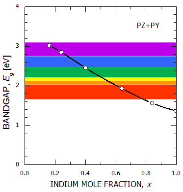
Bandgap (and color
emission) as a function of indium content
[K. Yalavarthi, SISPAD
2012] |
|
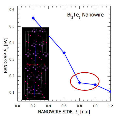
Multiscale Design of Nanostructured Thermoelectric Coolers
: Here, our objective is to deploy a multiscale simulator
for thermoelectric cooler devices, where the material parameters are
obtained atomistically using a combination of molecular dynamics and
tight-binding simulations and then used in the system level design.
In a recently published work [A. Sharmin, M. Rashid, V. Gaddipati,
A. Sadeque, and S. Ahmed, “Multiscale Design of Nanostructured
Thermoelectric Coolers: Effects of Contact Resistances,” Journal of
Electronic Materials, in press, DOI: 10.1007/s11664-014-3520-8,
November 2014], after benchmarking the simulator against a recent
experimental work [I. Chowdhury, R. Prasher, K. Lofgreen, G.
Chrysler, S. Narasimhan, R. Mahajan, D. Koester, R. Alley and R.
Venkatasubramanian, “On-chip cooling by superlattice-based thin-film
thermoelectrics”, Nature Nanotechnology, vol. 4, pp. 235–238, 2009],
we carried out a detailed numerical investigation of the performance
of Bi2Te3 nanowire based thermoelectric devices for hot-spot
cooling. The results suggest that active hotspot cooling of as much
as 23 ºC with a high heat flux is achievable using such
low-dimensionality structures. However, it has been observed that
thermal and electrical contact resistances, which are quite large in
nanostructures, play a critical role in determining the cooling
range and lead to significant performance degradation that must be
addressed before these devices can be deployed in such applications.
Besides applications in embedded and potable coolers, thermoelectric
devices are used as power sources for remote telecommunication,
navigation, and radioisotope generator for space vehicles, and show
great promise in heat scavenging in vehicle exhaust system.
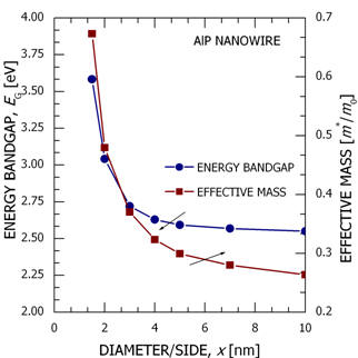
Recently, within a sp3d5s* tight-binding scheme, we have
determined the bandstructure of Bi2Te3
nanowire for use in high-temperature thermoelectric devices.
Previously, we worked on bulk Bi2Te3 material
(left panel of the below Figure). Right panel of the Figure shows
(inset) a rectangular (atomistic) Bi2Te3
nanowire having dimensions of Lx = 0.8 nm Ly = 0.8 nm, and Lz =
3.045 nm, and the energy bandgap vs. nanowire dimension
(side-length) plot where a decrease in bandgap with the reduction of
nanowire dimension is due to the quantum-mechanical
size-quantization effect.
[Supported by NSF] |
|
 |
 |
go to top
Nanoelectronics Software/Tools Development
|
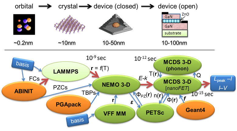
Software Development for Multiscale Modeling of
Conventional and Emerging Devices:
This work aims to develop a multiscale
Quantum Atomistic Device Simulator (QuADS 3-D) where: a)
material parameters are obtained atomistically using
first-principles, b) structural relaxation and phonon dispersions
are studied via molecular mechanics/dynamics, c) a variety of
tight-binding models (s, sp3s*, sp3d5s*) are used for the
calculation of electronic bandstructure and interband transition
rates, and d) coupled charge-phonon transport is simulated using a
combined Monte Carlo-NEGF framework. The atom-by-atom simulation
capability in QuADS 3-D exposes new degrees-of-freedom at nanoscale
(such as engineering the stress, hybrid crystal cuts, composition,
surface polarization, and electrostatics) and creates transformative
design routes for boosting performance and reliability of novel
nanoelectronic devices. QuADS 3-D uses several novel,
memory-miserly, parallel and fast algorithms [5], and incorporates
state-of-the-art fault-tolerant software design approaches, which
enables the simulator to assess the reliability of available
petaflop computing platforms (TeraGrid, NCCS, NICS). A web-based
online inter¬active version for educational purposes will soon be
available on http://www.nanoHUB.org.
[Shaikh Ahmed, Mohammad Rashid,
Saad Al-Qahtani, Md Rezaul Karim Nishat, Khadija Khair, Ye Wu,
Abdussamad Muntahi, Mayada Taher and Abdulmuin Abdullah, “Multiscale
and Multiphysics Modeling of Non-Classical Semiconductor Devices,”
ICECE 2016, Proc. of 9th Int. Conference on Electrical and Computer
Engineering, Dhaka, Bangladesh, December 2016.
(DOI:10.1109/ICECE.2016.7853846;
http://ieeexplore.ieee.org/document/7853846/)]
[Shaikh Ahmed, Krishnakumari Yalavarthi,
Vamsi Gaddipati, Abdussamad Muntahi, Sasi Sundaresan, Shareef
Mohammed, Sharnali Islam, Ramya Hindupur, Dylan John, And Joshua
Ogden, “Quantum Atomistic Simulations of Nanoelectronic Devices
using QuADS,” Nano-Electronic Devices: Semiclassical and Quantum
Transport Modeling, Springer, Book Edited by D. Vasileska and S. M.
Goodnick, pp. 405, 2011.] |
|
|
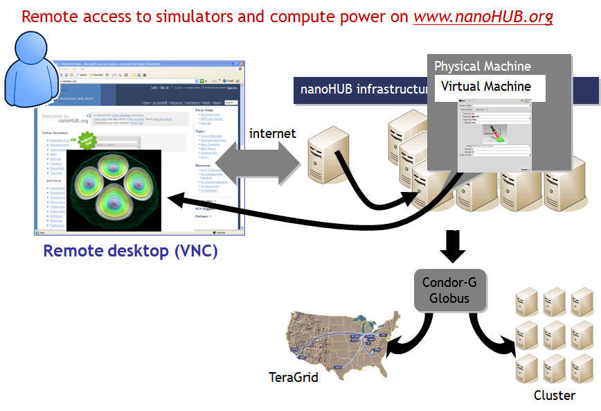
Community nanotechnology software
development: freely available on www. nanoHUB.org
The NSF Network for Computational Nanotechnology (NCN)
supports the National Nanotechnology Initiative through research, simulation
tools, and education and outreach. Deployment of these services to the science
and engineering community is carried out via web-based services, accessible
through the nanoHUB portal http://www.nanoHUB.org. The educational outreach of
NCN is realized by enabling access to multimedia tutorials, which demonstrate
state-of-the-art nanodevice modeling techniques, and by providing space for
relevant debates and scientific events. The second purpose of NCN is to provide
a comprehensive suite of nano simulation tools, which include electronic
structure and transport simulators of molecular, biological, nanomechanical and
nanoelectronic systems. Access to these tools is granted to users via the web
browsers, without the necessity of any local installation by the remote users.
The definition of specific sample layout and parameters is done using a
dedicated Graphical User Interface (GUI) in the remote desktop (VNC) technology.
The necessary computational resources are further assigned to the simulation
dynamically by the web-enabled middleware, which automatically allocates the
necessary amount of CPU time and memory. The end user, therefore, has access not
only to the code, a user interface, and the computational resources necessary to
run it but also to the scientific and engineering community responsible for its
maintenance. The nanoHUB is currently considered one of the leaders in science
gateways and cyber infrastructure. The process of web-based deployment of these
tools is depicted in the following Figure. A user visits the www.nanohub.org
site and finds a link to a tool. Clicking on that link will cause our middleware
to create a virtual machine running on some available CPU. This virtual machine
gives the user his/her own private file system. The middleware starts an
application and exports its image over the Web to the user’s browser. The
application looks like an Applet running in the browser. The user can click and
interact with the application in real time taking advantage of high-performance
distributed computing power available on local clusters at Purdue University and
on the NSF TeraGrid or the open science grid. I have been a contributor in this
well-established and long-term national nanotechnology initiative. In my
teaching of graduate and undergraduate level courses, I make extensive use of
these freely-available resources available from NCN. |
 |
 |
go to top
|